
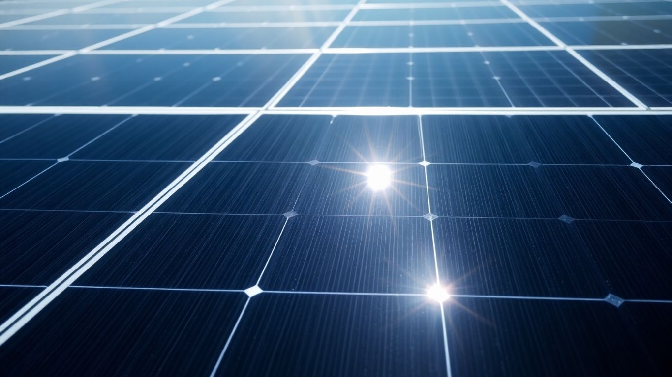
Facing current energy challenges, thin-film solar panels are emerging as an innovative alternative to conventional photovoltaic technologies. By integrating seamlessly into various sectors, these panels reveal astonishing potential. Their design is based on advanced manufacturing technology, which allows for the creation of lightweight and flexible structures, suitable for diverse environments. When compared with traditional systems, their distinct advantages quickly become clear. In the residential sector, they transform architecture by adding a sustainable and aesthetic dimension. As for commercial and industrial spaces, they promote optimised implementation of energy space. So, how do thin-film panels adapt to these different needs? Explore with us the specific features of this promising technology through an overview of applications dedicated to residential, commercial, and industrial particularities.
Key Takeaways on Thin Film
- Thin-film technology uses very thin semiconductor materials, measuring from a few nanometres to a few tens of micrometres, making them lighter and more flexible than conventional crystalline silicon cells.
- Manufacturing processes such as chemical or physical vapour deposition allow for the creation of these thin layers, paving the way for various architectural applications, including on complex or old structures.
- Thin-film panels excel in low-light conditions and offer potential for reduced production costs, while being suitable for uses such as semi-transparent glazing or facade integration.
- The main technologies on the market include cadmium telluride (CdTe), copper-indium-gallium-selenide (CIGS), and amorphous silicon (a-Si), each with its own performance and cost characteristics.
- Although their current market share is lower than that of crystalline silicon, thin-film solar panels are experiencing significant projected growth, with active research aimed at improving their efficiencies and expanding their future applications.
Understanding thin-film photovoltaic technology
Thin-film solar cells represent a significant evolution in the field of photovoltaic energy. Unlike older technologies based on crystalline silicon, they use layers of semiconductor materials of considerably reduced thickness, often only a few nanometres to a few micrometres. This thinness gives the panels remarkable lightness and flexibility, opening the way for architectural and structural applications previously unimaginable.
These devices are manufactured by depositing these active layers on various substrates, such as glass, plastic, or metal. This manufacturing method allows for great adaptability and opens up interesting prospects for integration into building elements or lightweight structures. The objective is to produce electricity from sunlight in a more economical and versatile way.
A thin-film solar cell, sometimes called a photovoltaic film, is a second-generation technology in the solar field. It is characterised by the application of one or more very thin layers of semiconductor materials on a support. These materials are chosen for their ability to convert sunlight into electricity. The main components of a thin-film cell typically include:
- The photovoltaic material: This is the heart of the cell, the semiconductor that absorbs photons and generates electrons. Common examples include cadmium telluride (CdTe), amorphous silicon (a-Si), or CIGS (Copper-Indium-Gallium-Selenide) type compounds.
- A conductive sheet: This layer, often metallic, ensures the collection of generated electrical charges and minimises energy losses.
- A protective coating: An external layer, usually made of glass or resistant plastic, protects the internal components from weathering and physical damage, thus ensuring the durability of the module.
The main innovation lies in the drastic reduction of the amount of active material required compared to conventional technologies, which directly impacts costs and application possibilities.
The most striking difference between thin-film technologies and traditional crystalline silicon solar panels lies in their thickness. While crystalline silicon cells use wafers that can reach 200 micrometres (µm), the active layers in thin-film cells are often in the order of a few nanometres (nm) to a few tens of micrometres. This reduction in scale is a major advantage.
| Technology | Typical active layer thickness | Common substrate | Flexibility | Approximate weight per m² |
|---|---|---|---|---|
| Crystalline Silicon (c-Si) | 150 – 200 µm | Glass | Rigid | 10-15 kg |
| Thin Film (e.g. CIGS) | 1 – 5 µm | Glass, Plastic, Metal | Flexible/Rigid | 2-5 kg |
This difference in thickness results in much lighter panels and, in many cases, flexible ones, which considerably expands the range of possibilities for integration.
Several types of semiconductor materials are used in the manufacture of thin-film cells, each having specific properties that determine their performance and applications. The most commonly used on the market are:
- Cadmium Telluride (CdTe): This material offers good light absorption and recognised stability, with relatively low production costs.
- Amorphous Silicon (a-Si): This is a non-crystalline form of silicon. Although its efficiency is generally lower than that of crystalline silicon, it is cheaper to produce and can be deposited on flexible substrates.
- Copper-Indium-Gallium-Selenide (CIGS): This family of materials exhibits some of the highest conversion efficiencies for thin-film technologies, approaching those of crystalline silicon. However, they are more complex to manufacture.
- Gallium Arsenide (GaAs): Although very high-performing, its high cost primarily reserves it for space or niche applications requiring exceptional efficiencies.
Manufacturing processes for thin-film solar panels
The manufacture of thin-film solar panels uses sophisticated deposition techniques to create high-performance and lightweight photovoltaic devices. Unlike traditional solar panels that use thick silicon wafers, thin-film technologies apply extremely thin semiconductor layers to a substrate. These processes allow for great flexibility in the choice of materials and supports, opening the way for various architectural and industrial applications.
Chemical Vapour Deposition (CVD) is a commonly used method for manufacturing thin-film solar cells. This process involves reacting precursor gases in a high-temperature reaction chamber. Atoms or molecules from the gases deposit on a heated substrate, thus forming a solid and uniform layer of the desired semiconductor material. CVD allows for good control over the thickness and composition of the layers, which is essential for optimising cell performance.
Physical Vapour Deposition (PVD), which includes techniques such as sputtering and thermal evaporation, is another key approach. In sputtering, an ion beam bombards a target of the material to be deposited, projecting atoms that then condense on the substrate. Thermal evaporation uses heat to vaporise the material, which then deposits on the substrate. These methods are particularly useful for depositing conductive metallic layers or specific semiconductor materials.
Cadmium telluride (CdTe) and copper-indium-gallium-selenide (CIGS) based solar cells are among the most mature thin-film technologies.
- For CdTe: Manufacturing often involves techniques such as sputtering to deposit the CdTe layer, followed by other deposition steps for the conductive and contact layers. Methods such as sublimation or vapour phase deposition are also used.
- For CIGS: The production of CIGS cells can be done by co-evaporation of copper, indium, gallium, and selenium, or by sputtering a precursor alloy followed by annealing in the presence of selenium and sulphur. The flexibility of the substrate allows for continuous production of solar cell rolls.
These processes, although complex, are optimised to allow for large-scale and lower-cost production, thus contributing to the attractiveness of thin-film technologies on the market.
Distinctive advantages of thin-film solar panels
Thin-film solar panels stand out significantly from more traditional photovoltaic technologies due to a set of advantages that considerably broaden their scope of application. Their unique design gives them properties that meet specific needs, both in terms of architectural integration and energy performance under various conditions.
Lightness and flexibility for varied integrations
One of the most striking benefits of thin-film panels lies in their reduced weight and their ability to bend. Unlike rigid crystalline silicon panels, which require robust and often costly mounting structures, flexible panels can be installed on curved or irregular surfaces. This opens up possibilities for integration on complex roofs, building facades, recreational vehicles, or even lightweight structures that would not support the weight of conventional panels. This adaptability greatly simplifies the installation process and reduces structural constraints. They are particularly well suited for mobile applications or on old buildings [0eba].
Performance in low-light conditions
A notable characteristic of thin-film technologies is their behaviour in reduced light. While crystalline silicon panels can see their electricity production drop significantly in cloudy, overcast weather or at dawn and dusk, thin-film panels maintain more consistent efficiency. They are able to capture a wider range of the light spectrum, including infrared and ambient light, which allows them to continue producing energy in conditions where traditional panels would be less efficient. This consistency is a significant advantage for maximising energy production over an entire day.
Potential for reduced production costs
The manufacture of thin-film solar panels generally uses fewer semiconductor materials than crystalline silicon-based panels. The processes for depositing these ultra-thin layers, although sophisticated, can potentially lead to a reduction in production costs on a large scale. Less raw material and simplified manufacturing processes can translate into a lower cost per watt, making solar energy more accessible. Although the initial cost may vary, the potential for decreasing manufacturing expenses is an important driver for their future adoption [e375].
All these advantages position thin-film panels as a versatile photovoltaic solution, capable of meeting integration and performance challenges that older technologies struggle to address.
Architectural and residential applications of thin films
Integration into complex facades and roofs
Thin-film solar panels are revolutionising the way we design buildings. Their flexibility and lightness allow them to be integrated onto surfaces that would be inaccessible to traditional solar panels. Think of roofs with unusual shapes or building facades that are not perfectly flat. These technologies adapt, offering an energy solution without compromising architectural aesthetics. This is a real opportunity to make every building, whatever its design, capable of producing solar energy.
Use in semi-transparent photovoltaic glazing
Another fascinating application concerns photovoltaic glazing. Imagine windows that produce electricity while letting light through. Thin films make this possible thanks to their ability to be semi-transparent. This opens up interesting prospects for office buildings or homes, where energy can be generated without sacrificing interior brightness. It is an elegant way to combine functionality and renewable energy production. The semiconductor materials used in these glazings are essential for this light-to-electricity conversion [1a97].
Adaptability to lightweight and old structures
One of the great advantages of thin-film panels is their low weight. This makes them particularly suitable for structures that could not support the weight of conventional solar panels. Old buildings, with more fragile frameworks, or lightweight constructions can thus benefit from solar energy. This adaptability considerably broadens the scope of possibilities for installing photovoltaic systems, allowing for easier and less structurally restrictive integration [361c]. Installation on roofs that are not ideally oriented, such as those that are not perfectly clear or south-facing, also becomes more feasible [eb2c].
Use of thin films in commercial and industrial sectors
The adoption of thin-film solar panels is experiencing a notable boom in the commercial and industrial spheres. These technologies offer an advantageous energy solution, particularly for businesses seeking to optimise their costs and reduce their ecological footprint. Their lightness and flexibility open up new installation possibilities on various structures.
Optimisation of space on corrugated factory roofs
Corrugated roofs, common in industrial complexes, pose a challenge for the installation of conventional solar panels. Thin-film systems, thanks to their adaptability, can be fixed to these surfaces without requiring major structural modifications. This allows for efficient exploitation of large areas, transforming industrial roofs into renewable energy production plants. This approach facilitates integration without compromising the integrity of the building.
Exploitation of vast spaces in logistics depots
The vast flat roofs of logistics depots represent considerable potential for solar energy production. Thin-film panels can be easily deployed there, maximising solar coverage. Their increased performance in low-light conditions is a major asset, allowing for more consistent energy production throughout the day and year. Installation on these sites contributes significantly to the energy autonomy of businesses.
Contribution to the energy transition of businesses
The integration of thin-film solar panels into commercial and industrial activities is a concrete step towards energy transition. It not only reduces electricity bills but also strengthens the company’s brand image as a player committed to sustainable development. These installations can improve the return on energy investment, an aspect increasingly scrutinised by investors. Thin-film cells show a better energy return on investment (EROI) compared to crystalline silicon cells, reaching 12 versus 10 for crystalline silicon, which highlights their long-term efficiency.
The adoption of these technologies allows businesses to meet growing demands for environmental responsibility while achieving substantial savings on their energy expenditure. It’s a win-win strategy for the economy and the planet.
The main advantages for the sector include:
- Reduction of operating costs through local energy production.
- Improvement of the overall energy efficiency of facilities.
- Enhancement of brand image through visible ecological commitment.
- Installation flexibility on diverse structures, including old or less robust roofs.
The study of new materials, such as lead-free perovskites for photovoltaic cells, promises to further improve the performance and durability of these systems [587e]. These technological advances strengthen the potential of thin films for industry.
Main thin-film technologies on the market
The landscape of thin-film photovoltaic technologies is diverse, although certain sectors have established themselves in the industrial market. These technologies are distinguished by the use of semiconductor materials deposited in very thin layers, offering specific advantages over crystalline silicon, which still largely dominates the market. Cadmium telluride (CdTe), copper-indium-gallium-selenide (CIGS), and amorphous silicon (a-Si) are the three main thin-film technologies currently produced on an industrial scale.
Cadmium telluride (CdTe)
CdTe is a thin-film technology that has gained popularity due to its good stability and relatively low production cost. Its manufacture involves depositing layers of cadmium telluride on a substrate. Although cadmium is a toxic element, modern manufacturing processes and recycling systems aim to minimise environmental impact. CdTe panels are often used in large solar power plants.
Copper-indium-gallium-selenide (CIGS)
CIGS cells represent another promising thin-film technology. They use a mixture of copper, indium, gallium, and selenium. These cells offer some of the highest conversion efficiencies for thin-film technologies, sometimes approaching those of crystalline silicon. Their flexibility allows for varied applications, including integration into building materials. However, their production cost can be higher than that of CdTe.
Amorphous silicon (a-Si)
Amorphous silicon (a-Si) is a non-crystalline form of silicon. It was one of the first thin-film technologies to be commercialised, particularly for small electronic applications such as calculators. a-Si panels are flexible and perform well in low-light conditions. However, their efficiency is generally lower than that of CdTe and CIGS technologies, and they can degrade more quickly under intense sunlight. The French market, for example, is seeing significant growth in solar installations, with a strong interest in innovative solutions [9c71].
It is important to note that, despite advances, thin-film technologies still represent a minority share of the global market compared to crystalline silicon [d459]. However, their potential in terms of flexibility, lightness, and architectural integration continues to drive research and development.
Performance and characteristics of thin-film cells
Thin-film solar cells, although thinner, exhibit distinct performance characteristics compared to their crystalline silicon counterparts. Their unique design allows them to stand out in certain operating conditions.
Conversion efficiencies compared to crystalline silicon
In general, thin-film technologies show slightly lower conversion efficiencies than crystalline silicon. Typically, a difference of 2 to 3 percentage points is observed. For example, while crystalline silicon can achieve high efficiencies, thin-film cells such as CdTe, CIGS, or amorphous silicon fall within a slightly lower range. However, it is important to note that significant advances have been made, with research achieving promising efficiencies for thin-film solar cells.
Stability and durability of materials
Despite their thinness, thin-film solar panels are designed to be durable. They are generally composed of three main elements: the photovoltaic material itself, a conductive sheet, and a protective layer. The latter, often made of high-quality glass or plastic, helps protect the module from external elements, thus extending its lifespan. Their inherent flexibility can also contribute to their resilience against certain mechanical stresses.
Ecological impact of life cycle analyses
Life cycle analyses suggest that thin-film panels have a potentially lower ecological impact than crystalline silicon panels. Although they may be slightly heavier due to their structure (often sandwiched between two panes of glass), the reduced amount of semiconductor materials used in their manufacture is a key factor. This results in a smaller environmental footprint over their entire lifespan, from production to disposal. The use of less abundant materials and lower-temperature manufacturing processes also contribute to this ecological advantage. Early integration of these technologies into architectural design can maximise their overall environmental benefit, as in the case of semi-transparent photovoltaic glazing.
Market evolution and prospects for thin films
History of thin-film technology market share
Thin-film technologies have been around for some time, with early applications such as solar calculators powered by amorphous silicon. While their potential to surpass crystalline silicon was predicted, their market share has fluctuated. For example, in 2010, they accounted for approximately 15% of the global market, but this figure dropped to 4.5% in 2019. However, forecasts indicate significant growth, with a projected market of $23 billion by 2029, more than double its size in 2020.
Global market growth projections
The global market for thin-film solar panels is expanding rapidly. Analyses predict substantial growth in the coming years, driven by technological innovation and increasing demand for flexible and lightweight renewable energy solutions. This growth is particularly visible in the commercial and industrial sectors, where their adaptability to existing structures and their performance in low-light conditions are major assets.
| Year | Estimated Market Share (in billions USD) |
|---|---|
| 2020 | 11.3 |
| 2029 | 23.0 |
Potential to surpass conventional technologies
Thin-film solar panels present considerable potential to compete with, or even surpass, conventional crystalline silicon-based technologies. Their lightness and flexibility allow for architectural applications and integration on various surfaces where rigid traditional panels are not suitable. Furthermore, continuous research aims to improve their efficiency and reduce production costs, which could strengthen their market position in the long term. The lower ecological impact, measured by life cycle analyses, is also a factor increasingly taken into account by consumers and industrialists.
The growing adoption of thin films in BIPV (Building-Integrated Photovoltaics) applications and their adaptability to complex industrial roofs underscore their relevance in the overall energy transition.
Innovations and future research in thin films
The field of thin-film photovoltaics is constantly evolving, with active research aiming to push the boundaries of performance and cost. Advances in semiconductor materials are opening up exciting new avenues for the future of solar energy.
Developments in semiconductor materials
Research focuses on exploring new materials capable of improving light absorption and conversion efficiency. Perovskites, for example, are attracting considerable interest due to their potential to achieve high efficiencies at low cost. The LOCAL-HEAT project, funded by the EU, is specifically working on the development of these next-generation perovskite materials to make clean energy more accessible. Other avenues include the use of organic materials and quantum dots, which could offer increased flexibility and lightness, paving the way for unprecedented applications.
Improving efficiencies and reducing costs
The main objective of research is to reduce the cost per watt while increasing cell efficiency. This involves optimising manufacturing processes, such as depositing more uniform and defect-free layers. Improving cell structure, particularly the design of contacts and passivation layers, also plays a key role. At the same time, research into cheaper and more durable substrates, as well as reducing the amount of active materials needed, contributes to lower production costs. A better understanding of semiconductor physics allows for optimising cell design, much like improving the quality of the wafer for traditional cells.
New emerging applications for thin films
Beyond traditional applications, thin films open the door to innovative uses. Their flexibility and lightness allow for their integration into smart textiles, portable electronic devices, or even complex architectural structures and vehicles. The development of semi-transparent thin films could revolutionise photovoltaic glazing, transforming windows into energy sources. The goal is to make solar energy ubiquitous and discreet, integrating harmoniously into our daily environment.
Technical considerations for installing thin-film panels
The installation of thin-film solar panels, although often simpler than that of traditional systems, requires particular attention to certain technical details to guarantee performance and longevity. It’s not just about fixing them; one must consider the environment in which they operate.
Protection against solid-borne noise
Thin-film panels, due to their lighter and sometimes more exposed nature, can be sensitive to vibrations and noise transmitted by the supporting structure. It is therefore recommended to provide damping systems or insulating fixings to minimise the transmission of sound waves. This may seem anecdotal, but prolonged exposure to vibrations can, in the long term, affect the reliability of electrical connections or even damage the semiconductor layers. A preliminary study of the acoustic environment of the installation site is therefore good practice.
Choice of equipment adapted to site specificities
The choice of fixing materials and cabling must take into account the specific environmental conditions of the site. For example, in areas with high salinity or UV exposure, corrosion and degradation resistant materials should be chosen. The flexibility of thin-film panels allows their integration on curved surfaces, but this imposes constraints on mounting systems that must adapt without creating excessive stress points. Thermal management is also important; although less sensitive to heat than crystalline silicon, good ventilation remains a key factor in maintaining optimal efficiency. The use of specific adhesive tapes for non-perforating installations, for example, requires validation of their durability over time and under different climatic conditions. For large-scale projects, a comparative analysis of different solar panel technologies can inform the choice of the most appropriate materials.
Integration from the architectural design phase
Optimal integration of thin-film panels occurs from the earliest stages of architectural design. This allows full advantage to be taken of their lightness and flexibility. For example, they can be integrated directly into facade or roofing elements, thus reducing the need for complex and costly support structures. This approach also allows for better anticipation of aesthetic and functional aspects, such as orientation to maximise solar exposure or managing shadows cast by other building elements. Close collaboration between architects, installers, and manufacturers is therefore essential for successful integrations.
- Careful planning: Evaluate the allowable structural load and choose appropriate fixings.
- Cable management: Provide protected and weather-resistant cable routes.
- Maintenance: Design the installation to facilitate access for future maintenance.
Anticipating technical and environmental constraints from the design stage is key to a successful and durable installation of thin-film solar panels, thus guaranteeing their long-term performance.
To install solar panels, a few important details need to be considered. For example, how best to fix them so they withstand wind and rain? Or, what is the best place for them to receive as much sun as possible throughout the year? These questions are crucial for your installation to work well and last a long time. If you want to know more about the technical aspects and how we can help you, visit our website to discover all the solutions we offer.
A promising energy future thanks to thin films
In summary, thin-film technologies represent a significant advance in the field of photovoltaics. Their flexibility, lightness, and adaptability open up unprecedented integration possibilities, whether in building architecture or on less conventional surfaces. Although their market share is still developing compared to established technologies, their potential for innovation and their contribution to a more diversified energy transition are undeniable. The continuous evolution of these technologies promises increasingly efficient and accessible solutions to meet tomorrow’s energy challenges.
Frequently Asked Questions
What is a thin-film solar panel?
Imagine a super thin solar panel, much lighter than the ones you usually see. It’s made by stacking tiny layers of special materials that capture sunlight to make electricity. It’s a bit like a very thin pancake but one that produces energy!
How are these panels made?
Special techniques are used to deposit these thin layers of materials onto substrates like glass, plastic, or even metal. It’s a bit like printing very fine images, but with materials that capture the sun.
Are they as efficient as normal panels?
They are a little less efficient than large silicon panels, but they have a great advantage: they work better when there isn’t much sun, like on cloudy days. And they are easier to install on surfaces that aren’t flat.
Where can these panels be used?
Anywhere where classic panels are too heavy or too rigid! They can be placed on building facades, in windows (sometimes transparent!), on curved roofs, or even on older structures that wouldn’t support the weight of normal panels.
What materials are used in these panels?
The best known are very thin silicon (amorphous silicon), cadmium telluride (CdTe), and copper-indium-gallium-selenide (CIGS). Each has its own little secrets for effectively capturing light.
Are thin-film panels lighter?
Yes, that’s one of their biggest assets! Because they are very thin, they weigh much less than conventional solar panels. This makes them easier to transport and install, especially on roofs that aren’t very strong.
Are they cheaper to manufacture?
Generally, yes. Since less material is used and manufacturing processes can be faster, the production cost can be lower. This is good news for making solar energy more accessible.
Can they be folded?
Absolutely! That’s the magic of thin film. Some of these panels are so flexible that they can be rolled or folded. This opens up incredible possibilities for integrating them into objects or structures that move or have original shapes.